Impedance Matching (for Voltage/Current/Power)
For your design, you will likely be using ideal input sources and a load capacitor for your block testing. However, your block will usually be hooked up between other blocks so for accurate performance, you need to take this into account for your design.
Standard Two-Port Model
Figure 1 shows the standard two-port model with voltage gain :

Figure 1: Standard Two-Port Model
Now, suppose we hook up an actual source voltage (with source impedance) and load impedance as shown in Figure 2.
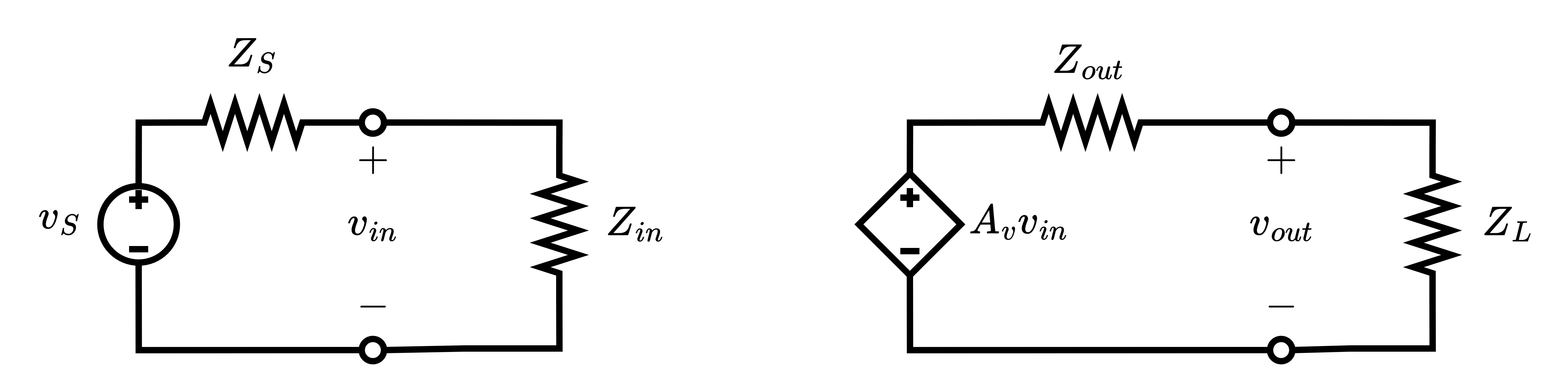
Figure 2: Standard Two-Port Model with Source and Load
If we calculate , the voltage on the load, in terms of , the ideal voltage source into the system, we get:
Notice the voltage dividers here! Ideally, we would want , but we must consider the input and output impedance of the two-port in our calculations.
Suppose we have to hook up two blocks together; the two-port model would look something like Figure 3.

Figure 3: Cascaded Two-Ports
Important: Here we have illustrated the considerations for voltage amplifiers, but similar considerations must be made for current amplifiers and hybrid amplifiers (transconductance, transimpedance); you will have current dividers for the inputs/outputs that are being processed as currents (this is essentially the same parallel as Thevenin/Norton equivalence).
General Design Principles
How do you design the input and output impedances of your circuits such that integrating your block with other blocks doesn’t impact performance? The table below is a general table describing the ideal impedances such that loading doesn’t occur for different types of amplifiers:
| Type of Amplifier | Input Type | Output Type | Ideal | Ideal |
|---|---|---|---|---|
| Voltage-Voltage | Voltage | Voltage | ||
| Current-Current | Current | Current | ||
| Transimpedance | Current | Voltage | ||
| Transconductance | Voltage | Current |
Table 1: Optimal Impedances
While this may seem like a lot more stuff to consider, for CMOS systems, some of these considerations can be relaxed. For example, for reasonably low frequencies, CMOS transistors can be approximated to have infinite input impedance, which is ideal for voltage input so it may be okay to have a high output impedance to drive a CMOS transistor (be careful with this for higher frequency systems because there is still capacitance to consider that could present a low input impedance at these frequencies; essentially, having a high output resistance could result in low bandwidth when trying to drive the capacitance of the next stage).
Important: When thinking about the input and output impedance of your amplifier, you must take into account the feedback network you are using for your circuit. For example, how do you make a transimpedance amplifier (TIA) using CMOS transistors with approximately infinite input impedance? A TIA will usually use shunt-shunt feedback which lowers both your input and output impedance (since your feedback network is in parallel with your input and output) so your actual input impedance won’t be that high. If you use the correct feedback structure, it will usually improve your input/output impedance characteristics for the type of amplifier you are building so take advantage of this!
Power Match
For RF communications systems, the act of transmitting and receiving a signal using antennas is one that involves the power of the signal rather than the voltage or current independently (the strength of an electromagnetic wave in free space is related the power delivered to the antenna; when you receive this signal, the power is very low and since this is what ultimately determines the SNR, you should avoid power loss as much as possible).
Consider Figure 4, which is a circuit model where the antenna is modeled as a voltage source in series with a resistance (representing a power source) and the input impedance at the start of your Rx chain is the load for the antenna.
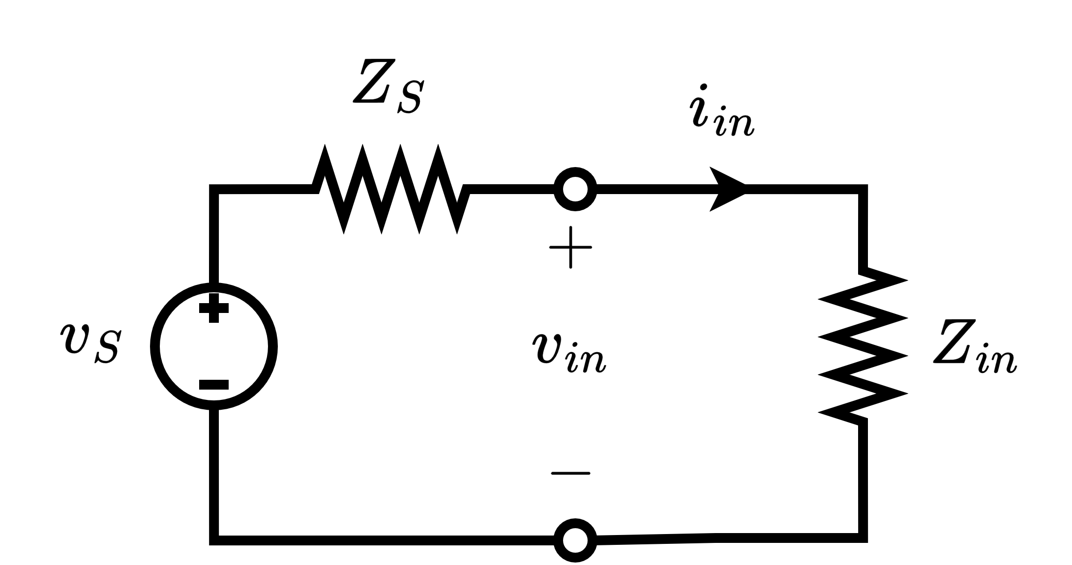
Figure 4: Antenna Drive Model
If you want to deliver maximum power to , there is a balance between having low (for more current) and having high (for a higher voltage divider ratio). So what’s the optimal ? Here’s the expression for power delivered to :
The maximum of this expression occurs at ; this is called a conjugate match (or maximum power transfer). The standard impedance for transmission lines (and antennas) in the vast majority of systems is , which is why in RF contexts you will often hear about “matching to .”
Okay, assume we have a system, so we ideally want for maximum power transfer. How does that factor into our design? You can’t/shouldn’t alter your block design since the sizing for that is designed for particular parameters needed for that block’s specs. To match to your desired impedance, you design a matching network (using inductors and capacitors at resonance) to change the impedance looking into your block into , like shown in Figure 5 (the exact structure will depend on the impedance values, but it will be some shunt/series LC network).

Figure 5: Antenna Drive Model with Matching Network
The exact math behind matching networks will be left to your RFIC classes, but there are many calculators that can help you design your match.
The factor of your match is important particularly for communications where you have a bandwidth around which modulation occurs (so you need a passband that supports that bandwidth). There are ways to make lower matches (e.g., two-stage match) or higher matches (e.g., matches / T matches) that you can explore if that is important for your application (note that inductor factors on chip are around at best so this is a limitation if you are trying to make a higher match; your maximum inductance is also limited by area so keep this in mind as well).